


Analog Devices Inc. ADL5205アンプ
Analog DevicesADL5205は、広い帯域幅、デジタル制御された可変デュアルゲインアンプ(DGA)として設計されています。 Analog Devices高速シリコンゲルマニウム(SiGe)補完BiCMOSプロセスを使用して開発されたADL5205には、正確なゲイン調整機能があり、優れた歪み性能が備わっています。 ADL5205には、正確なゲイン制御、最初の12dBの減衰のためのほぼ一定のノイズ指数、高出力3次インターセプト(OIP3)が備わっています。 ADL5205の48.5dBm OIP3性能によって、ADL5205は、レシーバアプリケーション用の優れたゲイン制御デバイスです。 ADL5205 DGAには、広い入力ダイナミックレンジアプリケーション用の1dBステップサイズがある広い35dBのゲイン範囲が備わっています。 複数のゲイン制御およびインターフェースオプションを介してゲイン調整が可能です。 これらのオプションには、並列、SPI、ゲインステップアップ/ダウン制御があります。 ADL5205の典型的な自己消費電流は、高性能モードで175mA、低消費電力モードで135mAです。 無効にすると、ADL5205はわずか14mAしか消費せず、優れた入力/出力間の絶縁が備わっています。 アンプは、デバイスを無効にするとゲイン設定が有効になります。
特徴
- Dual, independent, digitally controlled gain amplifier(DGA)
- -9dB to +26dB gain range
- 1dB step size, ±0.2dB accuracy at 200MHz
- 100Ω differential input resistance
- 10Ω differential output resistance
- 1.2dB change in noise figure for first 12dB of gain reduction
- Output third-order intercept (OIP3): 48.5dBm at 200MHz, 5V, high-performance mode
- −3dB bandwidth: 1700MHz typical in high-performance mode
- Multiple control interface options
- Parallel 6-bit control interface with latch
- Serial peripheral interface (SPI) with fast attack
- Gain step-up/down interface
- Wide input dynamic range
- Low power mode
- Power-down control
- Single 3.3V or 5V supply operation
- 40-lead, 6mm × 6mm LFCSP package
アプリケーション
- Differential analog-to-digital converter (ADC) drivers
- High intermediate frequency (IF) sampling receivers
- High output power IF amplification
- Instrumentation
Functional Block Diagram

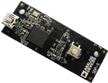
Evaluation Board

Analog Devices Inc. ADL5205-EVALZ評価ボード
ADL5205アンプの特性と機能を評価する設計者に役立ちます。
Analog Devices Inc. Analog Devices EVAL-SDP-CS1Zコントローラーボード
SDP-Sコントローラボード; このボードを使用すると、構成、およびUSB経由PCからドーターボードでのデータの取り込みが可能になります。
公開: 2016-10-31
| 更新済み: 2022-03-11