


Infineon Technologies PSoC®4XX8_BLE組込みシステムコントローラ
Cypress Semiconductor PSoC® 4XX8_BLE組込みシステムコントローラには、組込みシステムコントローラ用のスケーラブルで再構成可能なプラットフォームがあります。 このコントローラには、プログラム可能で再構成可能なアナログ/デジタルブロックに柔軟性の高い自動ルート機能を組み合わせたARM® Cortex™-M0 CPUがあります。 PSoC 4XX8_BLEは、統合Bluetoothローエナジー(BLE)を搭載したマイクロコントローラとの組み合わせで、Bluetooth Smart、無線、サブシステム(BLESS)としても知られています。 一部の機能には、デジタルプログラマブルロジック、高性能、アナログデジタル変換(ADC)、オペアンプなどが含まれています。 PSoC 4XX8_BLE製品は、PSoC4プラットフォームのメンバーと互換性があり、新しいアプリケーションや設計ニーズに対応できます。
特徴
- 32-bit MCU subsystem
- 48MHz Arm Cortex-M0 CPU with single-cycle multiply
- Up to 256KB of flash with read accelerator
- Up to 32KB of SRAM
- BLE radio and subsystem
- 2.4GHz RF transceiver with 50Ω antenna drive
- Digital PHY
- Link-layer engine supporting master and slave modes
- RF output power: -18dBm to +3dBm
- RX sensitivity: -92dBm
- RX current: 18.7mA
- TX current: 16.5mA at 0dBm
- RSSI: 1dB resolution
- Programmable analog
- Four op amps with reconfigurable high-drive external and high-bandwidth internal drive, comparator modes, and ADC input buffering capability. Can operate in Deep Sleep mode
- 12bit, 1Msps SAR ADC with differential and single-ended modes; channel sequencer with signal averaging
- Two current DACs (IDACs) for general-purpose or capacitive sensing applications on any pin
- Two low-power comparators that operate in Deep Sleep mode
- Programmable digital
- Four programmable logic blocks called universal digital blocks (UDBs), each with eight macrocells and data path
- Cypress-provided peripheral component library, user-defined state machines, and Verilog input
- Power management
- Active mode: 1.7mA at 3MHz flash program execution
- Deep Sleep mode: 1.3µA with watch crystal oscillator (WCO)on
- Hibernate mode: 150nA with RAM retention
- Stop mode: 60nA
- Capacitive sensing
- Cypress Capacitive Sigma-Delta (CSD) provides best-in-class SNR (>5:1) and liquid tolerance
- Cypress-supplied software component makes capacitive sensing design easy
- Automatic hardware tuning algorithm (SmartSense™)
- Segment LCD drive
- LCD drive supported on all pins (common or segment)
- Operates in Deep Sleep mode with four bits per pin memory
- Serial communication
- Two independent run-time reconfigurable serial communication blocks (SCBs) with reconfigurable I2C, SPI, or UART functionality
- Timing and pulse-width modulation
- Four 16-bit timer/counter pulse-width modulator (TCPWM) blocks
- Center-aligned, edge, and pseudo-random modes
- Comparator-based triggering of kill signals for motor drive and other high-reliability digital logic applications
- Up to 36 programmable GPIOs
- 7mm × 7mm 56-pin QFN package
- 76-ball CSP and thin CSP packages
- Any GPIO pin can be CapSense, LCD, analog, or digital
- Two overvoltage-tolerant (OVT) pins; drive modes, strengths, and slew rates are programmable
- PSOC Creator™ Design Environment
- Integrated Design Environment (IDE) provides schematic design entry and build (with analog and digital automatic routing)
- API components for all fixed-function and programmable peripherals
Associated Products

Infineon Technologies CYBLE-212006-01 EZ-BLE™ XR WICED®モジュール
Bluetooth Low Energy (BLE) ワイヤレス通信のための完全認証・完全認定の取得と設計を実現しています。

Infineon Technologies CYBLE-202007-01 EZ-BLE™ XR WICED®モジュール
Bluetooth Low Energy (BLE) ワイヤレス通信のための完全認証および完全認定を取得しています。
Associated Board
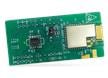
Infineon Technologies CYBLE-212006-EVAL EZ-BLE PROC評価ボード
EZ-BLE PRoCモジュール(CYBLE-212006-01)でのアプリケーションの評価と開発が可能になります。
Block Diagram

公開: 2016-04-25
| 更新済み: 2025-08-19