


Analog Devices / Maxim Integrated MAX32625 & MAX32626 32ビットMCU
Maxim Integrated MAX32625およびMAX32626 Arm® Cortex®-M4F 32ビット・マイクロコントローラは、ウェアラブル医療やフィットネスのアプリケーションの新興分野に最適です。このアーキテクチャは、超低電力、高効率信号処理機能、および使いやすさを兼ね備えています。内部96MHz発振器によって、高性能の機能を提供しています。内部4MHz発振器は、常時オンモニタリングを必要とするアプリケーションを対象に、最低限の電力消費に対応しています。MAX32625およびMAX32626 MCUは、512kBのフラッシュと160kBのSRAMを実現しています。これらのデバイスは、4つの強力かつ柔軟性の高い電力モードが特徴です。周辺機器管理ユニット(PMU)によって、最大6チャンネルでのインテリジェントなペリフェラル制御が可能になり、電力消費が大幅に削減されています。内蔵されたダイナミッククロックゲーティングおよびファームウェア制御によるパワーゲーティングによって、ユーザーは、特定のアプリケーション向けに電力を最適化できるようになります。
The MAX32625 and MAX32626 MCUs provide 512kB of flash and 160kB of SRAM. These devices feature four powerful and flexible power modes. A peripheral management unit (PMU) enables intelligent peripheral control with up to six channels to significantly reduce power consumption. Built-in dynamic and firmware-controlled clock gating allows users to optimize power for the specific application.
The Analog Devices MAX32625 and MAX32626 MCUs are available in WLP-63 and TQFN-EP-68 packages with a -30°C to +85°C operating temperature range.
View MAX32625EVKIT & MAX32626EVKIT Evaluation Kits
View MAX32625PICO Evaluation Board
特徴
- High-Efficiency Microcontroller for Wearable Devices
- Internal Oscillator Operates Up to 96MHz
- Low Power 4MHz Oscillator System Clock Option for Always-On Monitoring Applications
- 512KB Flash Memory (256KB “L” Version)
- 160KB SRAM (128KB “L” Version)
- 8KB Instruction Cache
- 1.2V Core Supply Voltage
- 1.8V to 3.3V I/O
- Optional 3.3V ±5% USB Supply Voltage
- Optimal Peripheral Mix Provides Platform Scalability
- SPI Execute in Place (SPIX) Engine for Memory Expansion with Minimal Footprint
- Three SPI Masters, One SPI Slave
- Three UARTs
- Up to Two I2C Masters, One I2C Slave
- 1-Wire Master
- Full-Speed USB 2.0 Device with Internal Transceiver
- Sixteen Pulse Train (PWM) Engines
- Six 32-Bit Timers and 3 Watchdog Timers
- Up to 40 General-Purpose I/O Pins
- 10-Bit Delta-Sigma ADC Operating at 7.8ksps
- AES -128, -192, -256
- CMOS-Level 32kHz RTC Output Available in All Power Modes
- Power Management Maximizes Uptime for Battery Applications
- 106μA/MHz Active Current Executing from Cache<
- 49μA/MHz Active Current Executing from FlashWake-Up to 96MHz Clock or 4MHz Clock
- 600nA Low Power Mode (LP0) Current with RTC Enabled
- 2.56μW Ultra-Low Power Data Retention Sleep Mode (LP1) with Fast 5μs Wake-Up on 96MHz Clock Source
- 27μA/MHz Low Power Mode (LP2) Current
- Secure Valuable IP and Data with Robust Internal Hardware Security (MAX32626 Only)
- Trust Protection Unit (TPU) Provides ECDSA and Modular Arithmetic Acceleration Support
- PRNG Seed Generator
- Physical Specifications
- Wide Operating Temperature: -30°C to +85°C
- Package Options
- WLP-63
- TQFN-EP-68
- RoHS Compliant
アプリケーション
- Sports Watches
- Smart Watches
- Fitness Monitors
- Wearable Medical Patches
- Portable Medical Devices
- Sensor Hubs
Development Tools
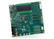
Analog Devices / Maxim Integrated MAX32625EVKIT/MAX32626EVKIT評価キット
MAX32625/MAX32626 MCUの機能の評価向けに、便利なプラットフォームを実現しています。

Analog Devices / Maxim Integrated MAX32625PICO評価ボード
FPUが搭載されたMAX32625 ARM Cortex-M4マイクロコントローラに基づく迅速な開発プラットフォームです。

Analog Devices / Maxim Integrated MAX32625MBED ARM mbed対応開発プラットフォーム
MAX32625マイクロコントローラの機能を評価するための便利なプラットフォームを提供します。
Block Diagram

Typical Application Circuit
